New in this snapshot: 7 drawings, 13 STEP files, 13 documents/media.
2026-10-19 8:44 PM ET — Open consideration: heavy parts inverted on bottom board
Mounting heavy components (e.g. transformers) hanging inverted on a bottom board needs review during the thermal/mechanical phase: anchoring (screws, straps, adhesive), solder-joint load, vibration, heat rising into the stack, and stack feet height. Deferred; noted only.
2026-10-19 8:45 PM ET — Open consideration: stack orientation
The stack may be mounted on its side (or other orientations), so the thermal/mechanical review must cover orientation: side loads on heavy parts and anchors, convection direction, standoff/pogo loading.
2026-10-20 8:08 AM ET — Design rule: ground pours
No separate inner ground plane (stay 2-layer). Both outer pours are ground; unused vias are tied to ground to stitch top and bottom and avoid floating islands. Stitch densely near the pogo block and along signal traces.
2026-10-20 8:10 AM ET — Note: grounding rules in spec-to-object
Pinout and routing will include automated grounding rules (ground pin placement and count, return paths, stitching) as part of spec-to-object programming.
2026-10-20 8:11 AM ET — Future idea: conductive multi-material interposer
Someday a multi-material 3D print with conductive features could contact ENIG ground features on the boards. Parked as too complex for now.
2026-10-20 8:14 AM ET — Signal path length and buses
At stack scale (worst case ~0.3-0.5 m), no bus (UART, I2C, SPI, CAN, RS-485, SPE) is length-limited. Concerns are protocol-specific and go into layout/design rules for spec-to-object: I2C capacitance per crossing, fast SPI edges/timing, impedance for USB HS/SPE (keep on-board or cable), and optional per-board termination for multi-drop buses (CAN/RS-485).
2026-10-20 8:18 AM ET — Decision: via-in-pad on companion lap pads
Companion lap pads get plated via-in-pad (~Ø0.4–0.6) with an exposed top ring so solder wicking confirms each blind joint visually; add extra paste. Logged in PENDING_ADJUSTMENTS.md for the next batch.
2026-10-20 8:33 AM ET — Request: DIY mini wave / dip solder pot for the OSSO 140x140 blanks
- the designer wants a concept design: pot size and solder mass, heater, PID control, an optional wave, dross handling, a masking carrier/tray, lift and depth stop, and safety. Deliverables: drawings, STEP, BOM, journal.
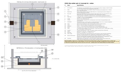
2026-10-20 8:42 AM ET — Solder pot v1 (concept A: full-size dip pot) + mask trays
- Files:
- drawings: wave_pot_v1_geom.py (writes wave_pot_v1.json); wave_pot_v1.py → wave_pot_v1.png (plan + section + notes), wave_pot_v1_p2.png (trays + BOM), wave_pot_v1.pdf (both pages).
- cad/wave_pot_v1: make_wave_pot_v1.py, wave_pot_v1_assembly.step, wave_pot_v1_tray_top_v1h.step, wave_pot_v1_tray_base_v3b.step, BOM_wave_pot_v1.md.
- Decision rationale: a small static pot with the board traversing it does not work. L2 must sit 0.5 below the solder surface while the pot rim is above it, so a wider tray hits the rim. Traversing needs a raised wave (concept B, a v2 option).
- Concept A, the dip pot:
- Cavity 160x160x30, rim +5 above the working solder surface, solder depth 25 = 640 cm³ → SAC305 4.72 kg / Sn63 5.38 kg.
- The tray displaces 56 cm³, raising the level by 2.2 mm.
- 6 x 250 W cartridges in a steel block = 1.5 kW. Heat-up ≈ 15 min (1.26 MJ, pot 6.3 kg). Idle loss ≈ 250 W.
- Concept B, mini wave: pot 180x70x50, 441 cm³ → SAC305 3.25 kg.
- Mask trays: Durostone, 150 sq lower box, 210 sq flange, 140.4 pocket, 2.0 web.
- Top v1h: 20 apertures, 7283 mm² open. Every one of the 1028 grid + 22 strip lands is fully exposed. Masked features are at least 0.3 away (SMT 0.3, pogo 2.31, window 1.87).
- Base v3b: 2 apertures for the 48 holes.
- Fiducials A/B are left open, because masking them would create floating islands; they get a Kapton dot.
- STEP reimport: assembly 0.91 MB, 37 solids, valid. Trays are 1 solid each.
- Open decisions: D1 A vs B; D2 alloy; D3 pot material; D4 230/120 V; D5 peel tilt; D6 preheat; D7 fiducial dots; D8 nitrogen.
2026-10-20 9:12 AM ET — Request: design pivot to a perpendicular card-edge PSU companion
- The top-board companion changes to a vertical card that plugs into an EDAC 305-020-521-202 (2x10, 3.96 mm pitch, 5 A per contact).
- The card hosts a 10–15 W PCB-mount AC-DC module.
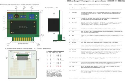
2026-10-20 9:18 AM ET — card_edge_psu_companion_v1
- Module: MEAN WELL IRM-15-5. Datasheet PDFs for IRM-15 and IRM-10 are in refs/psu_modules/, with SUMMARY.md.
- Card: 64 x 58 x 1.57 FR4 with a 43.2 finger tab.
- 18 gold fingers (9+9) at 3.96 pitch.
- Key slot at position 10/L, 1.40 x 8.01, for the in-contact key 307-240-328.
- Contact assignment: +V on 1,2,A,B; GND on 3,4,5,C,D,E; +V sense on 6/F; R_ID to GND on 7/H; 8,9,J,K not connected.
- Mains:
- Mains terminal, fuse and MOV at the top left; optional output terminal and test points at the top right.
- Mains pads clear the fingers by 9.5 and low-voltage pads by 8.84 (rule ≥ 6).
- Top-board placement (concept only):
- Connector centred at (70, 116.5). It sits entirely inside the current v1h window, so it needs the window, wings, lap pads and anchors removed (v1i).
- Not applied; PENDING_ADJUSTMENTS untouched.
- STEPs in cad/card_edge_v1 (all reimport valid):
- Companion with connector: 0.88 MB, 52 solids.
- Connector alone: 0.36 MB.
- Assembly on top v1h: 28.0 MB, 2297 solids; bbox z -1.54 to 64.08.
- Unverified: fuse and MOV values, finger width and length, contact lettering, key part number.
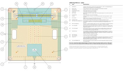
2026-10-20 9:34 AM ET — Top board v1i (card-edge family, variants A/B)
the designer approved this at 9:26 AM ET.
- PENDING applied:
- 8:30 lower-centre block becomes SMT-4: a NO-TH pour at x 51.0–89.0, y 12.0–44.14, merged with SMT-2B. 144 grid holes removed; 884 remain (v1h had 1028). Clearances: 0.75 to the strip lands, 0.42 to the kept grid lands, 1.5 to the pogo pads.
- 8:18 via-in-pad: superseded/N/A, because the top companion lap pads are gone. It may still apply to the base v3b companion laps.
- Future to-dos (wave pot, reflow, pick-and-place): not touched.
- Removed: the v1h window (main opening, centre tab, wings), 32 lap pads, 4 M2 anchors and the companion outlines.
- SMT-5 card-edge field: that area is now a NO-TH pour (x 25.5–114.5, y 94.5–140). It is SMT, not grid, because:
- The grid already stopped at y 92.86 under the old companion.
- The neighbours (SMT-2T, SMT-3 L/R and the fid no-grid zones) are all SMT.
- The 3.96-pitch connector rows and mounting holes cannot share the 2.54 lattice.
- Fiducials: not moved.
- Pin-1 silk void: moved +6.5 to y 127.5–133.5, because the CE-B ears overlapped it.
- CE-A: EDAC 305-020-521-202 (2x10) centred at (70,106).
- CE-B: EDAC 305-044-521-202 (2x22, verified on EDAC's site, drawing in refs/card_edge_396) centred at (70,120.5).
- Footprints: both have pin 1 at +x; PTH Ø1.3/Ø2.4 and mounting NPTH Ø3.3. CE-B ears reach into the fid no-grid zones; the mounting hole is 4.92 from the fid keep-out and the body 1.64.
- Shared pin map:
- Positions 1–10 are identical on both connectors: +V 1/A 2/B; GND 3/C 4/D 5/E; SENSE 6/F; ID 7/G; PG/RSV 8/H; RSV 9/J; KEY 10/K.
- 2x22 only: GND 11, 16, 21, 22; IO0–7 on the number row and IO8–15 on the letter row at 12–15 and 17–20.
- Lettering reconciled to EDAC (G is included; I and O are skipped). The PSU card geometry is unchanged.
- Variant A: card_edge_psu_v1 (IRM-15-5), rotated 180° so the module sits over SMT-5. The mains zone is 19.9 above board copper (rule ≥6).
- Variant B: blank card 100x58x1.57 with a 90.75 tab, 42 fingers and a key slot at position 10.
- Files:
- drawings: top_v1i_geom.py → top_v1i_geom.json; top_v1i.py → osso_top_v1i.png/.pdf.
- cad/top_v1i: make_top_v1i.py, VERIFY.txt, OSSO_top_v1i_board.step, OSSO_top_v1i_variantA_2x10_psu.step, OSSO_top_v1i_variantB_2x22_blank.step, OSSO_blank_card_2x22_v1.step. All re-import as valid.
- Open items:
- Body height: 11.68 on the part drawing vs 11.94 in the guide.
- Price/stock not verified.
- Finger dimensions are design values.
- The board is no longer symmetric about the connectors for bottom use.
2026-10-20 9:37 AM ET — Design note (the designer)
Top v1i card-edge footprints: the 2×10 and 2×22 are both optional per build. Either, both, or neither may be populated depending on component mounting; suppressing either carries no penalty.
2026-10-20 9:43 AM ET — Top v1i Variant C (5 mm terminal strip) + v8 freeze
- Variant C: the top v1i board with the 22-hole 5.0 mm strip at y=10 populated. The strip is two groups of 11 (x 15–65 and 75–125, with no hole at x=70). Each side gets 4× Phoenix Contact MKDS 1,5/ 2 (1715022) and 1× MKDS 1,5/ 3 (1715035), aligned with the side latch. That makes 10 blocks and 22 positions in total.
- Part data: 5.0 mm pitch, 9.8 mm long, 13.8 mm installed height, 0.9×0.9×3.5 pins, Ø1.3 hole (this matches the strip), M3 screws, 17.5 A / 400 V.
- Wire entry faces the bottom edge.
- CE-A 2×10 and CE-B 2×22 are NO-POP: the footprints stay, with no connector or card.
- Files:
- cad/top_v1i: make_variantC.py and OSSO_top_v1i_variantC_5mm_terminal.step. The STEP re-imports as valid (see VERIFY.txt).
- drawings/osso_top_v1i: has a Var C callout.
- Model note: this is a simplified envelope model. The pin row is assumed to be at the centre of the body depth.
- Freeze v8: versions/v8_2026-10-20 and OSSO_v8_2026-10-20.tar.gz.
- Contents: top v1i with the queued adjustments applied, the two-size card edge with the shared pin map, and Variants A, B and C.
- Both card-edge footprints are optional per build and can be suppressed without penalty.
- The 9:41 AM queued item (extend the three middle via columns to the strip) is NOT applied. It is carried as-is in PENDING_ADJUSTMENTS.md.