← v2 v4 →
v3: Process v3, alignment, blank spec, first Gerbers (blank v3b)
Frozen Fri Oct 16, 2026, 11:32 AM ET · 117 files · folder: versions/v3_2026-10-16/ · archive: OSSO_v3_2026-10-16.tar.gz
What changed
- Oct 16, 2026 10:46 AM ET: v3 process review, step 1 (fixturing and registration)
- Oct 16, 2026 10:48 AM ET: v3 process review, step 2 (silk removal)
- Oct 16, 2026 10:49 AM ET: v3 process review, step 3 (mask opening)
- Oct 16, 2026 10:51 AM ET: v3 process review, step 4 (in-place stencil)
- Oct 16, 2026 10:51 AM ET: v3 process review, step 5 (paste and stencil removal)
- Oct 16, 2026 10:52 AM ET: v3 process, renumbered
- Oct 16, 2026 10:53 AM ET: v3 process, steps 6b-10 (top-side components only for now)
- Oct 16, 2026 11:00 AM ET: v3 process compiled; alignment recommendations
- Oct 16, 2026 10:59 AM ET: Why top-side components only
- Oct 16, 2026 11:01 AM ET: In-circuit test (ICT) as a stack layer
- Oct 16, 2026 11:02 AM ET: No bare copper rule
- Oct 16, 2026 11:04 AM ET: PINNED, open item
- Oct 16, 2026 11:05 AM ET: Cleaning after mask reveal
- Oct 16, 2026 11:08 AM ET: v3a alignment proposal drawing
- Oct 16, 2026 11:12 AM ET: v3 concept A (alignment changes adopted)
- Oct 16, 2026 11:14 AM ET: Companion board design note (future)
- Oct 16, 2026 11:15 AM ET: Tuning priorities
- Oct 16, 2026 11:17 AM ET: Blank copper weight
- Oct 16, 2026 11:20 AM ET: Blank spec decisions
- Oct 16, 2026 11:22 AM ET: v3 concept B (Ø3.0 pogo pads, blank spec)
- Oct 16, 2026 11:24 AM ET: First Gerber prep (PCBWay upload test)
- Oct 16, 2026 11:30 AM ET: First Gerber set, OSSO BLANK v3b (PCBWay upload test)
- Oct 16, 2026 11:30 AM ET: v3b Gerbers, pin-1 mark restored
- Oct 16, 2026 11:32 AM ET: Via size
- Oct 16, 2026 11:32 AM ET: VERSION 3 FROZEN
New in this snapshot: 14 drawings, 0 STEP files, 2 documents/media.
Key decisions
Drawings new in v3
Other images
STEP files (0)
Documents & media
Journal entries in this version
Oct 16, 2026 10:46 AM ET: v3 process review, step 1 (fixturing and registration)
the designer: the blank mounts in a jig hard-mounted to the laser optical table. A microscope camera fixed rigidly to the galvo is zoomed on the blank registration mark, and the operator adjusts the jig screws while watching a large video display.
OSSO notes: (1) a fixed camera sees one point, but correcting rotation needs at least 2 widely spaced marks, so the jig must translate between marks or the camera offset must be known; (2) the 140mm blank in the 150mm field leaves about 5mm per side, so the alignment budget is tight; (3) double-sided engraving needs a datum visible from both sides, so consider drilled or plated reference holes (e.g. the corner M3s) rather than surface-only fiducials.
Oct 16, 2026 10:48 AM ET: v3 process review, step 2 (silk removal)
the designer: the engraver removes all silkscreen that should not remain (the inverse of the silk image). The ENIG pads are not silk-covered, so they are excluded, along with cutouts and drills.
OSSO notes: (1) on the blank, the silk must stop about 0.2mm short of all ENIG pads (pogo, corner rings, companion lap pads); (2) laser settings must remove silk without damaging the soldermask, which needs a laser test; (3) the removal image = board outline minus kept silk, pads, cutouts and drills, which can be auto-generated by the Spec-to-Object tool.
Oct 16, 2026 10:49 AM ET: v3 process review, step 3 (mask opening)
the designer: remove the soldermask everywhere copper must be exposed for SMT mounting.
OSSO notes: (1) mask opening comes before copper isolation, so the jig must hold registration between steps; (2) the new openings are bare copper (not ENIG) and need soldering soon, flux or OSP to avoid oxidation; (3) a mask-ablation laser test is needed, and openings should be about 0.05-0.1mm larger than the pads.
Oct 16, 2026 10:51 AM ET: v3 process review, step 4 (in-place stencil)
the designer: apply a flexible adhesive stencil film to the PCB and laser-cut the paste areas.
OSSO notes: (1) the stencil is self-registered, which is a big advantage; (2) use about 0.1-0.13mm polyimide/Kapton-type film (it sets the paste height) with clean peel and no residue; (3) a film-cut laser test is needed so cuts don't mark the exposed copper; (4) paste windows about 90% of pad area, and pogo, corner and companion ENIG pads stay covered (no paste).
Correction (10:52 AM): companion lap pads likely DO get paste (soldered joint); only pogo and corner ENIG pads stay covered.
Oct 16, 2026 10:51 AM ET: v3 process review, step 5 (paste and stencil removal)
the designer: squeegee the paste through the film, then peel the stencil off.
OSSO notes: peel slowly at a low angle while the paste is wet; the jig must hold the board flat under squeegee pressure, and a film border helps the peel; the pogo and corner ENIG pads stay clean under the film.
Oct 16, 2026 10:52 AM ET: v3 process, renumbered
the designer added copper isolation after mask opening. Sequence: 1 fixture and register; 2 silk removal (inverse); 3 mask opening for SMT; 4 copper isolation (engrave negative outlines to define traces, rest stays as ground fill); 5 adhesive stencil film and paste-window cut; 6 paste, then peel stencil.
OSSO notes for step 4: cut goes through mask plus copper (laser test needed, passes depend on copper weight); about 0.15-0.2mm isolation gaps; ground fill ties to the - corner bus; clean debris before stencil film.
Oct 16, 2026 10:53 AM ET: v3 process, steps 6b-10 (top-side components only for now)
6b place components (jig camera can guide); 7 reflow, using a soak profile for the large ground-fill heat sink and keeping the board flat; 8 clean (IPA or wash), dry fully, keep ENIG pogo and corner pads bright; 9 inspect under the microscope camera, then continuity/short test (watch for slivers from isolation); 10 optional conformal coat or OSP on any remaining bare copper. Only top-side SMT for now, so a single reflow; the bottom side carries traces and pads only.
Oct 16, 2026 11:00 AM ET: v3 process compiled; alignment recommendations
- PROCESS_v3.md (and .pdf) has 13 steps: top silk, mask and copper; flip and repeat on the bottom; clean; stencil film; paste; place; reflow; clean; inspect and test; optional coat. It also lists the required laser parameter tests.
- Top recommendations:
- R1: a tooling hole (70,3.5) and slot (70,136.5) on the flip axis x=70, with dowels in the jig. The board self-registers on both sides, and the screws only trim.
- R2: a calibrated camera offset plus a known jig move, to measure rotation from 2 marks.
- R3: move the marks to about 22mm inward, as an asymmetric set.
- R4: plated fiducial holes, visible from both sides.
- R5: ENIG ring and dot marks.
- R6: galvo grid calibration and per-step verification crosses.
- R7: OpenCV crosshair overlay and auto-detection.
- Board changes: R1, R3, R4, R5, and the pin-1 and mirrored-mark clearance.
Oct 16, 2026 10:59 AM ET: Why top-side components only
the designer: components go on the top side only because of tight packaging interference within the stack. It is better to add another layer to the stack than to work around bottom-side parts. Someday simple low-profile passives could go on the bottom, but that complication is avoided for now.
Oct 16, 2026 11:01 AM ET: In-circuit test (ICT) as a stack layer
the designer: ICT can be done with a dedicated test PCB that temporarily acts as another stack layer, using the standard interposer. Extra ENIG test pads (not interposer pads) may be added to boards for this custom ICT. OSSO note: test pads must stay reachable, clear of the printed ring, columns and spine (or the test interposer gets matching holes).
Oct 16, 2026 11:02 AM ET: No bare copper rule
the designer: avoid bare copper. Every laser-exposed copper area gets solder via paste and reflow, including unused (no-populate) pads, which still get paste. All other pads must be ENIG from the factory. Process change: the stencil paste windows include no-populate pads; step 13 (optional coat/OSP) is dropped.
Oct 16, 2026 11:04 AM ET: PINNED, open item
Isolation-cut copper edges (bare sidewall on both sides, bottom never reflowed). Options discussed: conformal coat masked with laser-opened stencil film, or accept the edges and run tarnish tests. the designer may prefer other TBD methods. Unresolved.
Oct 16, 2026 11:05 AM ET: Cleaning after mask reveal
the designer: a cleaning step after the copper reveal lets the laser "just barely" get through. OSSO: IPA removes loose soot but not charred mask film; plan a stop-short laser pass, then IPA, then a light mechanical scrub (fiberglass pen or Scotch-Brite) or a mild flux wipe. Add the cleaning method comparison to the mask-off-copper laser test.
Status (11:06 AM): cleaning method after mask reveal is TBD and will be decided by laser testing.
Oct 16, 2026 11:08 AM ET: v3a alignment proposal drawing
- Script: drawings/align_proposal_v3a.py. Drawing: drawings/align_proposal_v3a.png. base_v2u.py is unchanged.
- Left side shows the current marks, with the 150mm field outline. Right side shows the proposal:
- Ø3.0 NPTH hole at (70,3.5), round dowel.
- 2.0x3.0 slot at (70,136.5), diamond dowel.
- Fiducials A (22,22) and B (118,22) as plated Ø0.3 holes with ENIG rings. They are each other's mirror, so the same holes register both sides.
- Fiducial C (118,112) on top. Its bottom mirror C' is at (22,112).
- Edge-stop zones on y=0 and y=140 (x 15-125), no-stop along x=0, Ø13 clamp keep-outs at the corner rings, and a 10mm distortion band.
- Detail D shows the fiducial design.
- Collision check found no conflicts:
- Edge vias: the hole and slot sit on x=70, which is skipped in the via rows. The nearest vias are at 64.92 and 75.08.
- Companions: C' keep-out edge is 2.5mm above the upper companion (top at y=107).
- Pin-1 is at least 7mm away. TH zones and the pogo block are clear.
- Notes:
- The hole and slot sit under the interposer ring band (0.5-6.5), so the printed ring must not have bosses there.
- The hole edge is 2.0mm from the board edge.
- A/B and their mirrors coincide by design.
- The current (128,128) mark mirrors onto the pin-1 triangle; the proposal removes this.
Oct 16, 2026 11:12 AM ET: v3 concept A (alignment changes adopted)
the designer accepted all of align_proposal_v3a (R1-R8). The v2 files are untouched.
- drawings/base_v3a.py → osso_base_v3a.png
- Fiducials A (22,22) and B (118,22) are Ø0.3 plated holes with an ENIG ring (2.0 outer / 1.0 inner). C (118,112) is a surface mark.
- Ø3.0 non-plated tooling hole at (70,4.0) and a 2.0x3.0 slot at (70,136.0). I moved them inward from 3.5, which gives a 2.5mm edge web with 1.5mm to the edge-via pads, still under the ring.
- New callouts 17-21: tooling hole, tooling slot, jig edge stops, no-stop edge at x=0, clamp keep-outs. Callout 14 updated and title changed to v3 concept A.
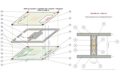
- drawings/osso_exploded_v3a.py → _p1.png, _p2.png and .pdf
- New fiducials and tooling hole/slot on both boards, plus new callout 24. The section callouts are renumbered 25-36.
- drawings/base_v3a_side.py → osso_stack_side_v3a.png
- New callout 10 for the jig no-stop edge (x=0) and callout 11 for the hidden tooling hole and slot.
- PROCESS_v3.md and .pdf
- Steps 1 and 5 now register on the dowel hole and slot plus fiducials A and B, which are visible from both sides. C (or C' on the bottom) is the orientation check.
- R1-R8 are marked ADOPTED.
Oct 16, 2026 11:14 AM ET: Companion board design note (future)
the designer: some companion boards may extend beyond the overall 140mm outline to allow large or specialty components. OSSO note: this affects the 150mm enclosure (it needs openings or a larger shell) and the no-edge-stop side at x=0.
Oct 16, 2026 11:15 AM ET: Tuning priorities
Most tuning expected: (1) SMT copper exposure (mask off without char or copper damage); (2) copper isolation (clean cut, no slivers or FR4 damage); (3) stencil film cut, which lands on freshly exposed bare copper and must not mark it (the designer). Silk removal is expected to be easier.
Oct 16, 2026 11:17 AM ET: Blank copper weight
Decision: blank uses 1oz (35um) copper. Remaining blank-only decisions: mask and silk color/type for UV ablation; thickness and ENIG spec; pogo pin and column width; drill and plating specs; what fixed silk ships on the blank.
Oct 16, 2026 11:20 AM ET: Blank spec decisions
- Mask: BLACK. Silk: WHITE, full coverage (removed areas reveal black; best camera contrast).
- Board 1.6mm FR4, 1oz copper, standard ENIG thickness.
- Pogo pads: generous, so a later pin change won't deprecate old base boards; OSSO recommends Ø3.0 ENIG (was Ø2.0), which fits the 5.08mm pitch.
- Drilling and plating per standards for now.
- Nothing preprinted: no logo or branding (open source spirit).
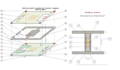
Oct 16, 2026 11:22 AM ET: v3 concept B (Ø3.0 pogo pads, blank spec)
- drawings/base_v3b.py → osso_base_v3b.png, copied from v3a.
- Pogo pads go from Ø2.0 to Ø3.0 ENIG. They are generous on purpose, so a later pin change does not make older boards obsolete.
- Clearance check: no via moves were needed.
- The channel vias sit at dx 5.08 / dy 2.54 from the pads: 5.68mm center to center, 3.68mm edge to edge to the Ø1.0 via pads.
- Pad to pad in a column (5.08mm pitch): 2.08mm.
- Between columns (10.16mm): 7.16mm.
- The pads fit inside the 4.6mm printed columns (0.8mm each side).
- Added a BLANK SPEC block to the notes:
- 140x140mm, 1.6mm FR4, 2-layer, 1oz copper.
- Standard ENIG, black mask, full white silk fill with no preprinted text or branding.
- Drills and plating per fab standard. I assumed the M2 anchors are non-plated; this needs confirming.
- Callout 9 and the title updated.
- drawings/osso_exploded_v3b.py → _p1.png, _p2.png and .pdf: the pads are Ø3.0 in the exploded view and in section A-A, with notes updated. The section column is drawn 4.0mm wide over the 3.0mm pad, which is fine.
Oct 16, 2026 11:24 AM ET: First Gerber prep (PCBWay upload test)
Confirmed: the M2 companion anchors are NPTH. Before generating, sizes still to set: via drill/pad, TH zone drill/pad, fiducial hole size (0.4mm suggested), M3 plated 3.2mm. Non-standard fab notes: full silk flood over copper (no clipping except pulled back from ENIG), full copper pour both sides fully masked, ENIG only on exposed pads, isolated pads in pour intentional, NPTH callouts, routed NPTH slot, tight tolerance on tooling datum, no order number or markings, single boards with no panel tabs.
Oct 16, 2026 11:30 AM ET: First Gerber set, OSSO BLANK v3b (PCBWay upload test)
- Script: fab/gen_v3b_gerbers.py (hand-written RS-274X X2 + Excellon; no KiCad on box). Output: fab/v3b_blank/, zip fab/OSSO_blank_v3b_gerbers.zip. Rendered back with gerbv: fab/render/*.png, preview fab/v3b_blank/OSSO_blank_v3b_preview_top.png.
- Layers: GTL/GBL, GTS/GBS (negative, openings), GTO/GBO (full flood), GTP/GBP (empty), GKO (outline + cutouts), PTH and NPTH drills (.TXT).
- Copper: full pour both sides, 0.3 pull-back from edge, cutouts, NPTH. Islands: pogo Ø3.0 in Ø4.0 clear (40, both sides); corner Ø7 in Ø9 clear; lap pads 2.0x1.0 with 0.4 gap (32, top); fiducials ring OD2.0/ID1.0 with Ø0.7 land on the Ø0.4 plated A/B holes, C top dot Ø0.3 at (118,112), C' bottom at (22,112); copper cleared to Ø4.0 around each fiducial so the mask-free area shows only the ring.
- Vias (71: 27 channel + 44 edge) and TH zones (48) tie directly into the pour (simplest; laser isolates later).
- Mask openings: pads +0.05 radial; fiducials Ø4.0. Silk flood pulled back 0.2 from openings/holes/edge/cutouts, Ø5.0 at fiducials. Pin-1 triangle and all text omitted (flood only).
- Outline: R4 corners per v3b (not square). Window 27x74 (R5) included as a routed CUTOUT: v3b callout 3 says "27x74 mm cutout", and the stack concept (wire route, companions bridging it, TH zones seen through it) depends on it. Set WINDOW_CUTOUT=False in the script if it should be solid. Wiring slot 12x26 (R4) is a cutout.
- Vias made 0.3 drill / 0.6 pad per this request; the v3b notes text still says Ø0.6/Ø1.0 (mismatch to resolve).
Oct 16, 2026 11:30 AM ET: v3b Gerbers, pin-1 mark restored
the designer: "no markings" means no labels or branding only; all alignment marks stay. Pin-1 triangle added as a silk VOID (black mask shows): top (13,127)-(19,127)-(13,121); bottom mirrored under the L-R flip at (127,127)-(121,127)-(127,121), so it reads top-left when the flipped board is viewed from its own side. Clearance: C/C' keep-outs end at y=114.5, corner clamp rings at x 130.5, top TH zone ends at y 99.7, so no collisions. Verified present: A (22,22), B (118,22) Ø0.4 plated + rings both sides; C (118,112) top; C' (22,112) bottom; tooling hole Ø3.0 (70,4.0); slot 2.0x3.0 (70,136.0). FAB_NOTES item 9 updated, zip regenerated, top/bottom previews refreshed.
Oct 16, 2026 11:32 AM ET: Via size
the designer accepted the 0.3mm drill / 0.6mm pad vias as used in the Gerbers. The v3b Gerber set is conceptual, for PCBWay pricing and technical verification. Drawing notes (Ø0.6/Ø1.0) to be corrected in the next drawing revision.
Oct 16, 2026 11:32 AM ET: VERSION 3 FROZEN
Snapshot: versions/v3_2026-10-16 (drawings, refs, fab, process, journal). Key: base_v3b plan, exploded_v3b plus section, side_v3a, PROCESS_v3, Gerbers OSSO_blank_v3b (PCBWay concept test). Blank spec: 1.6mm FR4, 1oz, ENIG, black mask, white silk flood, Ø3.0 pogo pads, dowel hole and slot, fiducials A/B/C. Everything after this is v4.